Table of Contents
Lab 2 - Sequential Circuits. The register.
Storing digital information
The flip-flop
The hardware elements which can store data can be implemented through sequencial circuits called flip-flops. They store the values depending on the input value and the clock cycle; the stored value can be changed only when the clock has reached another positive transition ( the rising edge of the signal, the moment where a signal goes from low to high). There are 4 major flip-flop types: D, T, SR and JK. Our target is the first one, since it is the one we will use later in our implementations. It is the most important and it is mainly used for the implementation of the registers inside CPUs (the smallest and the fastest memory unit inside the hierarhy).
Block diagram for the D flip-flop
The inputs and the outputs are:
D- the value (data) to be storedclk- the clock signal, considered as 'active' on the rising edge of the signalQ- the current state / value!Q- the inverted value
The functional equation for the flip-flop is Qnext ⇐ D, meaning that the next state (Qnext) of the flip-flop will only be dependent on the D input, the current state (Q) being ignored, as we can notice from the table below:
| D | Q | Qnext |
|---|---|---|
| 0 | 0 | 0 |
| 0 | 1 | 0 |
| 1 | 0 | 1 |
| 1 | 1 | 1 |
Transition table for the D flip-flop
along with the transition tables, we can have a better overview of our system's behavior by monitoring the waveform (timing diagrams), as illustraded in the next snapshop. Here we can observe how the output Q changes only on the front edge of the clock and takes the value of the input D.
Waveform
The register
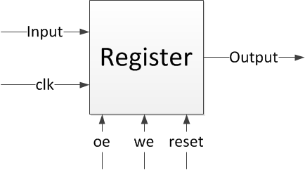
The flip-flop can store 1 bit of data. In order to extend the memory capacity, we can group several flip-flops together to store the data as a whole. When adding some controls and synchronizing the operations with the clock, we can call it a register. A register, like any other sequencial circuits, is sensitive to clk signal and shall also consider the reset, synchronus or asyncronus. In order to control the acces to a bus, the main operations shall be taken into consideration:
- reading - the current information is transported to the output of the module and put on the bus, controlled by
oe(output enable); - writing - the information which is currently on the bus shall be saved inside, controlled by
we(write enable).
The writing operation is synchronus; however, reading and reset can vary, depending on the usecase.
Exercises
In order to implement the exercises, use the lab archive below, considering the simulator you have on your workstation. The files already have a Xilinx ISE / Vivado project that you are able to run; in addition, for this practice you already have a testing module; the checking will be performed visually during the lab practice. Follow the instructions and hints below and the zones marked with TODO in the corresponding files.
Lab practice
- Implement the register, by analysing the block diagram above and the implementation delails below:
- read is asynchronus: when
oeis high, theoutshall imediatelly be activated with the stored data; - write is synchronus: when
weis high, the input data found on theinis stored; the effect are seen at the next clock cycle; - where should not be a dual access (write and read in the same time).
- Implement a simple counter, which increments it's value every clock cycle. The data shall be available to the output of the counter at any point.
Home assignment
NOTE: You can start the implementation using the files from the lab practice and modify them accordingly! The work files for this will be uploaded later this week, however they will not contain any major improvements.
- (5p) Implement another type of register, considering both write and read operations are synchronus. Add a new port, debug_output, as an output with the same size, that will always show the content of the register. Upload a screenshot to prove that the read operation generates the result on the positive edge of the
clksignal.- Hint: Synchronus operations are implemented in the sequencial blocks using the non-blocking assignments
⇐ - Hint: Use the implementation from the lab as reference.
- Hint: When adding the new port inside the working module register, don't forget to add it also in the test module!
- (5p) Starting from exercise 2 from the lab practice, implement an enchanted counter with 2 additinal inpus:
enable: 0 - counter is disabled (the value remains the same) 1 - counter is enabled (it counts up or down, depending on thedirection- see below)direction: 0 - counter increments it's value; 1 - counter decrement it's value- Hint: Use the implementation from the lab as reference.
- Hint: Add relevant stimuli to the testcase to exercise all the possible behavior. Upload a screenshot and put a short description to explain the behavior that it is shown.


